Master SMT Quality Control: 6 Critical Process Steps from Printing to Reflow
In electronics manufacturing, SMT (Surface Mount Technology) processing is the critical factor determining core product performance and reliability. From a bare board to component-dense circuitry, the entire workflow is deeply interconnected, where a lapse at any stage can trigger cascading failures. Industry statistics show that over $60\%$ of soldering defects originate during solder paste printing, while the reflow profile directly dictates final joint quality. This guide provides a comprehensive breakdown of the six critical control points from paste printing to reflow soldering, delivering an actionable quality management standard for electronics manufacturers.
Step 1: Solder Paste Printing — The Gatekeeper of SMT Quality
Solder paste printing serves as the starting point of the entire SMT process, dictating the success or failure of subsequent placement and soldering. Controlling the print stage equates to controlling $60\%\text{–}70\%$ of total soldering quality.
Stencil: The Precision Tool. Stencils act as the template for paste transfer; design and condition are critical. Thickness typically ranges from $0.1\,\text{mm}$ to $0.15\,\text{mm}$, with aperture tolerances controlled within $\pm 0.02\,\text{mm}$ and tension maintained above $25\text{–}35\,\text{N/cm}^2$. For fine-pitch devices like BGAs, “circular aperture with relief compensation” designs are standard practice.
Squeegee: The Uniform Applicator. Squeegees press paste through stencil openings onto PCB pads. Operating pressure ($50\text{–}120\,\text{N}$), speed ($20\text{–}80\,\text{mm/s}$), and angle ($45^\circ\text{–}60^\circ$) collectively determine deposition quality.
Solder Paste: The Raw Material. Solder paste requires cold storage at $2\text{–}10^\circ\text{C}$ and must naturalize to ambient temperature for $4\text{–}8\,\text{hours}$ before use. For fine-pitch components, Type 4 or finer alloy powders are strongly recommended.
Step 2: SPI (Solder Paste Inspection) — High-Precision Defect Detection
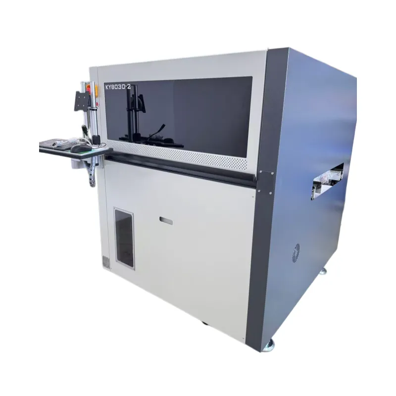
SPI functions as the primary quality gate post-printing, utilizing 3D optical measurement technology to conduct comprehensive pre-placement paste inspections.
Inspection Metrics: Precisely measures solder paste height, area, volume, and positional offset across every pad.
Acceptance Criteria: Paste height measuring below $75\%$ of stencil thickness or deviating beyond $\pm 25\%$ of target values is classified as defective. For ultra-miniature components like $0402$, deviations must remain within $10\%$.
Core Value: SPI intercepts defective print panels before downstream entry, feeding inspection data back upstream to optimize printing parameters and establish closed-loop control.
Step 3: Component Placement — The Intersection of Precision and Speed
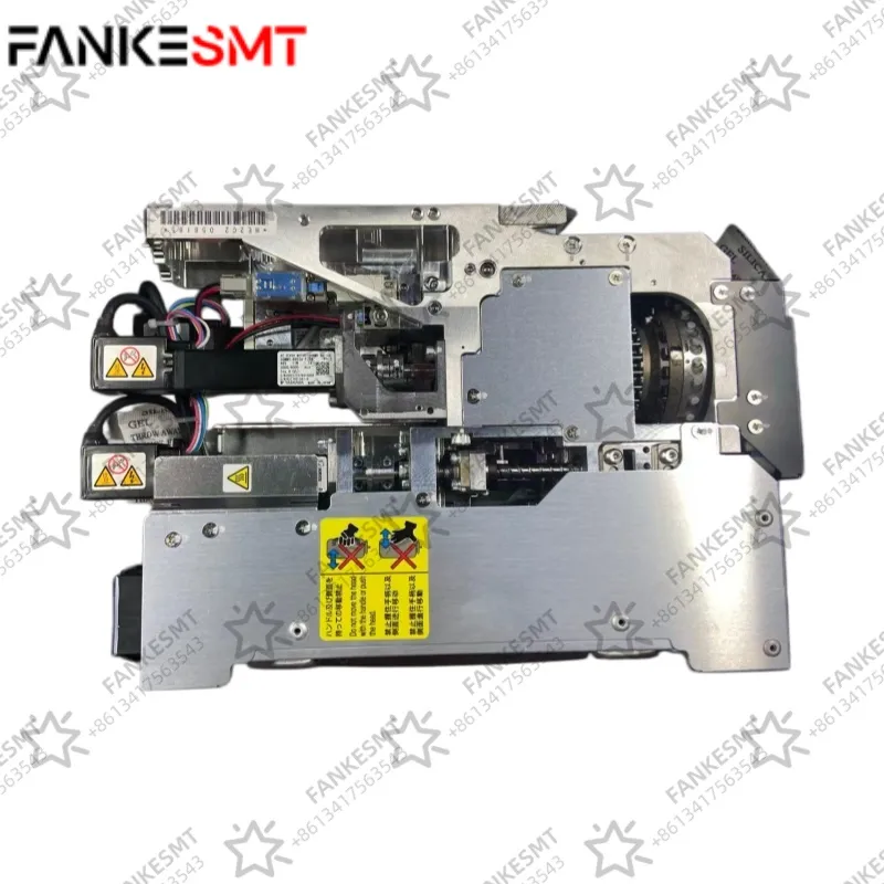
Placement systems anchor the SMT line, executing component pick-up, vision recognition, and micron-level placement within rapid cycle times.
Equipment Allocation: Lines typically deploy high-speed placers (handling massive volumes of passive chips) alongside multi-functional placers (handling complex BGAs, QFPs, and odd-form components) in tandem.
Accuracy Parameters: Standard component placement demands roughly $\pm 0.1\,\text{mm}$ accuracy, while high-precision packages like BGAs require up to $\pm 0.025\,\text{mm}$. Ultra-small components like $0201$ chips require placement accuracy within $\pm 50\,\mu\text{m}$.
Critical Details: Select matching nozzles based on component geometries (e.g., $0.3\,\text{mm}$ nozzles for $0402$ resistors) and guarantee precise feeder indexing (pitch accuracy down to $0.5\,\text{mm}$).
Step 4: Reflow Soldering — The Thermal Crucible for Permanent Bonding
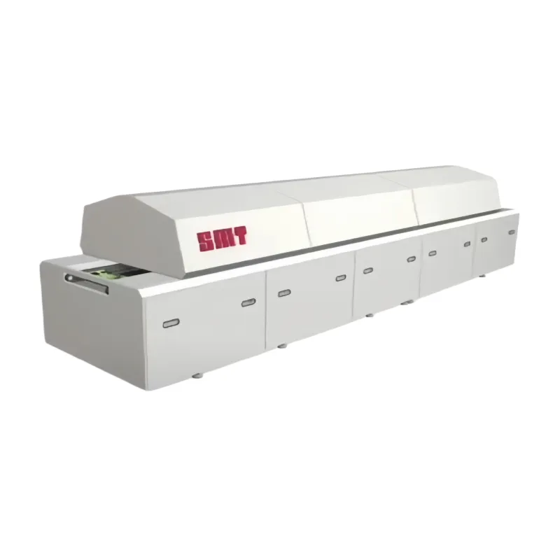
Reflow soldering is the core SMT process step, utilizing tightly managed thermal profiles to melt solder paste and establish robust joint integrity.
Standard Lead-Free Thermal Profile: Structured across four critical zones:
Preheat Zone: Elevates PCB temperature from ambient to $150\text{–}180^\circ\text{C}$ at a ramp rate of $1\text{–}3^\circ\text{C/s}$.
Soak (Thermal) Zone: Maintains $150\text{–}200^\circ\text{C}$ for $60\text{–}120\,\text{seconds}$ to fully activate flux chemistry.
Reflow Zone: Reaches peak temperatures of $235\text{–}250^\circ\text{C}$, keeping Time Above Liquidus (TAL) between $60\text{–}90\,\text{seconds}$.
Cooling Zone: Rapidly cools the assembly at $2\text{–}6^\circ\text{C/s}$ to solidify solder joints.
Critical Reminder: Every new product introduction mandates physical test board profiling to validate actual thermal performance against programmed targets. Running production without empirical profiling is a severe process control violation.
Step 5: AOI & X-ray Inspection — Dual Insurance for Quality Assurance
Post-soldering inspection relies on Automated Optical Inspection (AOI) and X-ray imaging to comprehensively evaluate structural and assembly quality.
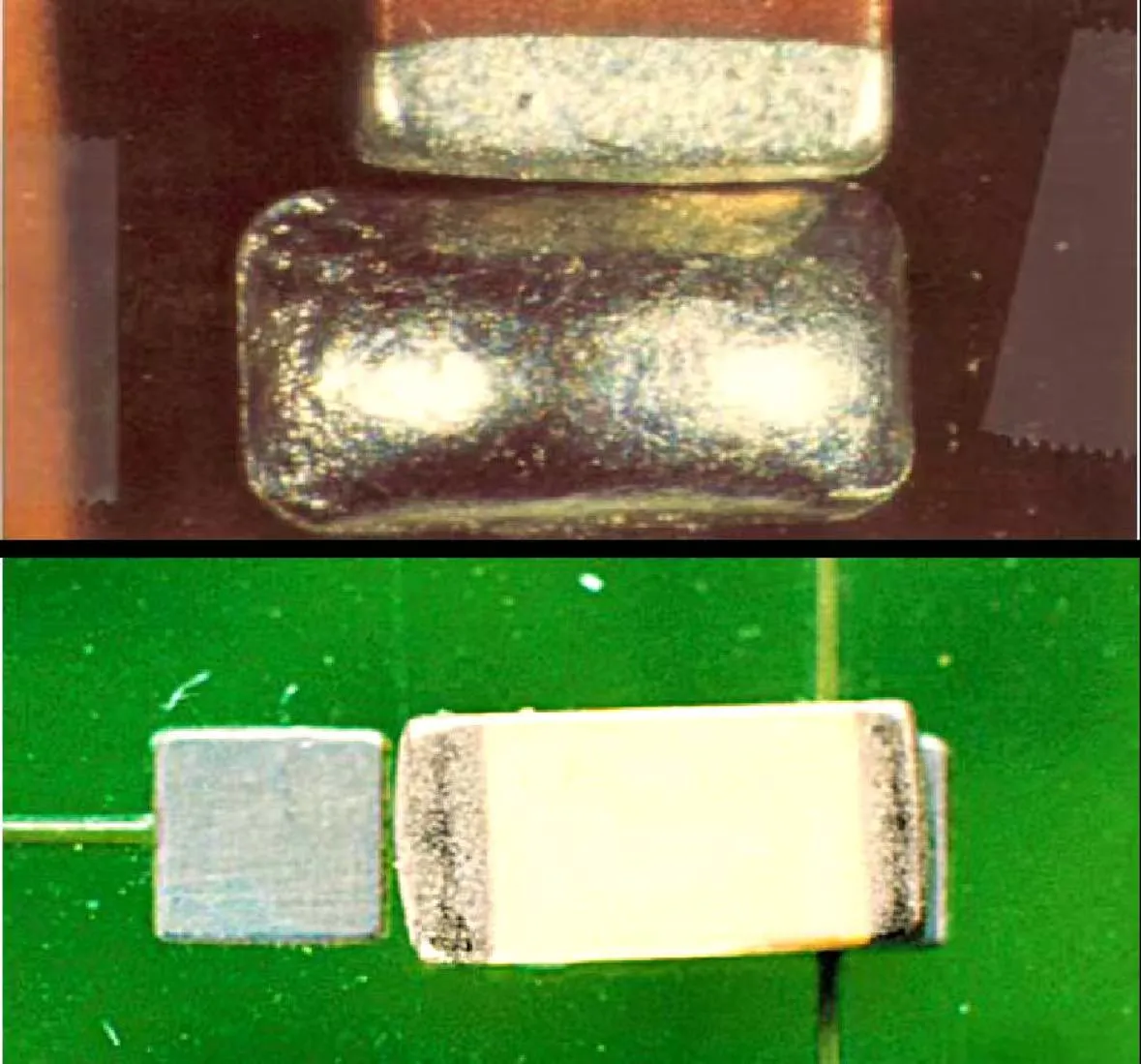
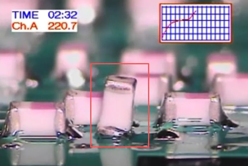
AOI Inspection: Employs optical scanning to rapidly identify surface-visible defects including component shifting, tombstoning, bridging, and insufficient solder. It serves as the primary surface quality safeguard.
X-ray Inspection: For bottom-terminated components like BGAs and QFNs where optical inspection fails, X-ray non-destructive testing provides complete subsurface visibility. It accurately identifies internal voiding, non-wetting, and cold joints within BGA solder balls. Per IPC standards, maximum single-joint voiding ratios for BGAs must generally stay below $25\%$.
Step 6: Testing & Packaging — Final Verification Prior to Delivery
Following core assembly and inspection, finished boards undergo electrical verification and packaging to ensure safe customer delivery.
Electrical Testing: ICT (In-Circuit Testing) isolates individual component parameters, while FCT (Functional Testing) simulates actual operating environments to verify total board functionality.
Cleaning & Packaging: Depending on process specifications, residual flux is cleaned from board surfaces. Assemblies are subsequently sealed in ESD-safe, moisture-barrier packaging to protect product integrity during transit and storage.
Conclusion
SMT processing is a complex system engineering discipline where final quality relies on the seamless collaboration of the entire workflow rather than any isolated step. From upstream solder paste printing and precision component placement to core reflow soldering and comprehensive AOI/X-ray evaluation, every phase safeguards product reliability.
For organizations pursuing high yields and uncompromising reliability, implementing Standard Operating Procedures (SOPs) spanning these six core control points—paired with rigorous first-piece inspection, inline monitoring, and closed-loop data feedback—is the definitive path to transforming SMT manufacturing from a game of chance into deterministic delivery.