SMT Placement Efficiency: Complete Design Guide to Fiducial (Mark) Points
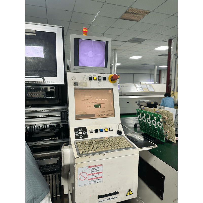
In electronics manufacturing, SMT placement machines achieve thousands of precise component placements per hour through the synergy of “brain and eyes”—where the “eyes” are fiducial (Mark) marks. Fiducial marks are optical reference patterns placed on the PCB surface to enable placement machines to determine board coordinates, position, and rotation angle. Functioning like the origin of a coordinate system, fiducials allow machines to automatically compensate for minor mechanical offsets. Without them, placement systems cannot accurately align with solder pads, leading to misalignments, skews, or placement failures.
However, many engineers treat fiducial design as an afterthought, unaware that this minor graphical marker dictates the efficiency and quality of the entire SMT production line.
1. How Fiducial Marks Work
The core function of fiducial marks is providing precise optical alignment and calibration baselines for automated equipment like SMT placers and AOI systems. Before component placement, the vision system scans the board’s reference points to calculate precise physical locations, rotational angles, and potential thermal warpage.
Without reference fiducials, placement systems cannot determine target coordinates. Furthermore, poor fiducial design impairs machine recognition. If traces, silkscreen text, or pads crowd the mark, the vision system fails to isolate its shape, triggering frequent machine alarms and forcing line stoppages.
A properly engineered fiducial enables millisecond-level recognition and positioning, whereas a poorly designed marker traps production lines in repeated recognition failures and downtime. That is the true performance gap.
2. Design Specifications: Why Details Drive SMT Success
Designing a fiducial involves much more than drawing a random circle. Compliant fiducials demand strict adherence across shape, dimensions, placement, solder mask clearance, and surface finish.
Shape: Solid Circles Are Mandatory
While squares and other shapes exist, solid circles offer optimal recognition precision and system compatibility. Circular geometry presents uniform visual features from all angles, ensuring stable recognition regardless of PCB rotation. Avoid irregular or segmented designs to maintain recognition stability. Industry standards specify a $1.0\,\text{mm}$ solid circular geometry.
Dimensions: $1.0\,\text{mm}$ as the Golden Standard
Fiducial sizing directly drives recognition reliability. Industry practice recommends a $1.0\,\text{mm}$ ($\pm 0.2\,\text{mm}$) solid circle, with minimum diameters of $0.8\,\text{mm}$ and maximum limits of $3.0\,\text{mm}$. Size variation across all fiducials on a single PCB must not exceed $25\,\mu\text{m}$, ensuring zero positioning drift during machine scanning transitions.
Placement: Diagonal Distribution at Maximum Separation
Fiducial layout governs placement accuracy. Standards require placing global fiducials at opposite diagonal corners, separated by the maximum possible distance along the primary diagonal axis.
Each individual board or panel must feature at least one compliant pair of fiducials, though three marks configured in an “L” shape with asymmetrical diagonal placement represent best practice. Three points yield superior translation and rotation calculation accuracy compared to dual-point layouts. Additionally, fiducials must maintain a minimum $5\,\text{mm}$ clearance from board edges (or at least along conveyor transport edges). When using edge-conveyored rails, avoid placing fiducials near clamping zones or tooling holes.
Solder Mask Clearance: Generous Openings Prevent Interference
Solder mask clearance (the green oil-free zone surrounding the mark) is strictly governed. Clearance diameters typically measure $2.0\,\text{mm}$. Because solder mask polymers reflect light and interfere with vision capture, clearances must exceed copper pad diameters by at least $0.5\,\text{mm}$. In space-constrained layouts, minimum clearances can drop to $1.5\,\text{mm}$, provided the copper pad exceeds $1.0\,\text{mm}$. Global panel and single-board clearances average $3.0\,\text{mm}$, while local fiducials utilize $1.0\,\text{mm}$ clearance rings.
Surface Finish: Flatness, Smoothness, and High Contrast
Fiducials are typically constructed from bare copper (protected by clear anti-oxidation coatings), immersion tin, or nickel-gold plating. Surfaces must remain exceptionally flat with smooth, clean edges and high chromatic contrast against surrounding backgrounds. Rough, oxidized, dark, or low-contrast finishes blind placement vision systems, triggering recognition failures.
3. Common Pitfalls in Fiducial Design
Pitfall 1: Traces and Silkscreen Crowding Mark Zones
Fiducials require clear “keep-out zones” free from silkscreen legends, routing traces, or extraneous graphics to prevent machine recognition errors.
Pitfall 2: Substituting Regular Pads or Vias for Dedicated Fiducials
Engineers sometimes repurpose existing component pads or vias as makeshift fiducials. Although contract manufacturers may occasionally accommodate this, dedicated fiducials are irreplaceable. Pad and via geometries, sizing, and surrounding environments violate optimal recognition criteria, degrading accuracy.
Pitfall 3: Arbitrary Sizing
Drawing arbitrary $0.5\,\text{mm}$ or $2.5\,\text{mm}$ circles introduces critical risks. Undersized marks elude vision systems; oversized marks trigger false categorization. Sticking to the validated $1.0\,\text{mm}$ standard prevents recognition penalties.
Pitfall 4: Neglecting Surface Protection
Oxidized or contaminated fiducial surfaces disrupt optical reflectivity. While minor blemishes can be wiped clean, severe degradation requires process corrections. Utilizing cleanroom assembly environments and automated blow-cleaning steps minimizes shop-floor contamination.
4. The Business Value of Optimized Fiducial Design
Investing minutes in careful fiducial design yields massive production returns:
Efficiency: Compliant fiducials secure instant first-pass recognition without manual intervention, preventing downtime, lost capacity, and labor overhead.
Precision: Global and local calibration achieves micron-level placement accuracy, eliminating shifts, skews, and rotational defects. Fine-pitch devices like QFPs ($\le 0.5\,\text{mm}$ pitch) and BGAs ($\le 0.8\,\text{mm}$ ball pitch) demand dedicated local fiducials adjacent to package corners to maximize precision.
Cost Control: Engineering optimal fiducials incurs zero material cost while preventing catastrophic batch scrap and extensive production line stoppages.
Conclusion
Measuring just $1.0\,\text{mm}$ in diameter, the fiducial mark serves as the coordinate origin for SMT assembly lines, directly controlling vision speed, placement accuracy, and uptime stability.
All fiducial engineering must strictly adhere to international standards including IPC-7351, IPC-A-610, and J-STD-001 governing position tolerances, pad dimensions, trace clearances, and board-edge offsets. Spending a few extra minutes on proper fiducial design during the layout phase eliminates days or weeks of volume production downtime.
Small markers drive massive efficiency—fiducials deserve the rigorous attention of every PCB layout engineer.