AOI vs. X-Ray Inspection in SMT Manufacturing: Comprehensive Application Analysis and Scientific Selection Guide
As zero-defect manufacturing becomes the ultimate pursuit in SMT assembly, the choice of inspection technology directly impacts product quality and customer trust. As the two core inspection methods on SMT lines, Automated Optical Inspection (AOI) and X-ray inspection each play irreplaceable roles. However, faced with equipment investments scaling into the millions, engineers often struggle with deployment dilemmas: which technology truly fits their production lines? This guide contrasts underlying principles, detection capabilities, and application scenarios to help enterprises make scientific, data-driven decisions.
1. Fundamental Differences in Technical Principles
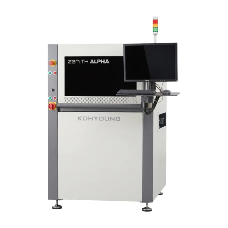
AOI (Automated Optical Inspection) is an optical imaging-based visual detection technology. It employs high-resolution industrial cameras paired with multi-angle lighting sources to capture surface images of PCBs, utilizing image-processing algorithms to compare them against standard templates. This identifies surface defects such as missing components, shifts, polarity errors, and solder bridging. Its essence is “seeing the surface”—relying on visible light reflection to inspect planar products.
X-Ray Inspection utilizes X-ray penetration characteristics to visualize internal structures. When X-rays penetrate materials of varying densities, absorption differences generate grayscale images—high-density solder joints appear bright white, while low-density substrates appear dark. Its essence is “seeing the interior”—penetrating packaging materials to reveal hidden solder joint states. One relies on visible light while the other uses X-rays; one inspects surfaces while the other fluoroscopes interiors—this represents their core divergence.
2. Detection Capability Comparison: Strengths and Limitations
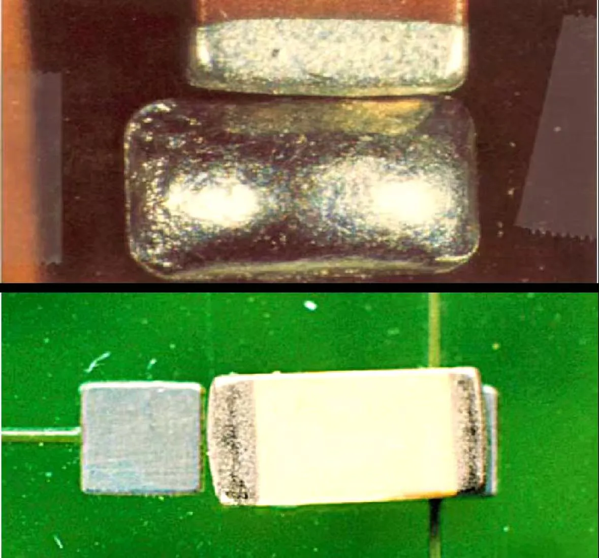
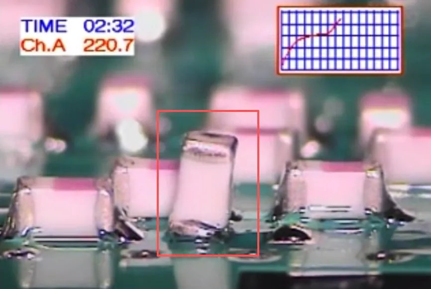
AOI excels in high speed, low cost, and broad coverage. It specializes in detecting surface-visible defects, including component omissions, misplacements, polarity orientation errors, solder bridging, insufficient/excess solder, and tombstones. Inspection speeds typically reach hundreds of joints per second, requiring only 10 to 20 seconds per board. AOI remains the most prevalent SMT inspection technology, accounting for over 60% market adoption.
Limitations: AOI cannot detect solder joints shielded by components or located underneath packages. For bottom-terminated packages like BGAs, QFNs, and CSPs, hidden joints completely escape AOI’s line of sight, leaving critical flaws like cold joints, non-wetting, and head-in-pillow (HIP) entirely undetected.
X-Ray bridges AOI’s blind spots precisely. It accurately identifies hidden flaws such as voids within BGA solder balls (voiding rates exceeding 25% severely compromise reliability), cold joints, bridging, opens, and HIP defects. X-ray achieves a defect capture rate exceeding 97% for process anomalies.
Limitations: High equipment costs (3D X-ray units range from $500,000 to $2,000,000), slower speeds (30 to 60 seconds per board), specialized operation requirements, and stringent radiation safety regulations.
3. Application Scenarios: When to Choose AOI vs. X-Ray
Primary AOI Scenarios: Typical applications include post-solder paste printing inspection, pre-reflow component placement inspection, and post-reflow final quality validation. Positioned across multiple line stages, AOI enables full-process monitoring. When products feature standard surface-mount devices (e.g., 0201, 0402, SOP, QFP), demanding high speed and cost-sensitivity, AOI is the prioritized choice.
Mandatory X-Ray Scenarios: Required when products incorporate bottom-ball packages like BGAs, CSPs, or flip-chips where traditional methods fail; for high-reliability failure analysis; or when customers explicitly mandate X-ray inspection reports. In automotive electronics, medical devices, aerospace, and defense, X-ray compliance is mandatory.
4. Scientific Selection and Configuration Strategies
In modern SMT environments, AOI and X-ray are complementary partners rather than mutual exclusives.
Standard Consumer Electronics: Prioritize AOI covering pre- and post-reflow stages, reserving X-ray strictly for first-article inspection (FAI) or custom customer mandates. According to IPC standards, consumer PCBs (Class 2) utilize “AOI + sampled X-ray.”
High-Reliability Products (Automotive, Medical, Defense): Implement combined AOI and X-ray deployments, utilizing full-line AOI alongside 100% or sampled X-ray penetration on critical devices. Medical and automotive PCBs (Class 3) mandate “full AOI + full X-ray verification.”
New Product Introduction (NPI): Prioritize X-ray during initial phases to optimize reflow profiles and stencil designs before固化 AOI parameters. Selection-wise, 2D X-ray suits rapid structural checks, whereas 3D CT excels in high-resolution volumetric analysis of fine-pitch joints.
5. Collaborative Quality Control: The MES Synergy
Integrating AOI and X-ray outputs into an MES smart manufacturing framework achieves closed-loop control across defect localization, root-cause analysis, and corrective actions:
First-Article Triple Verification: Synchronize manual visual inspection, AOI, and X-ray before batch production to confirm parameters.
Dynamic Process Sampling: Conduct scheduled AOI re-inspections and targeted X-ray scans mid-production to monitor stability.
Outgoing Quality Reports: Compile comprehensive defect distribution maps and X-ray joint screenshots to establish an unassailable quality evidence chain.
Conclusion
AOI excels at “fast and broad surface scanning,” while X-ray wins at “deep and transparent internal visualization.” Rather than substitutes, they form a golden partnership of distinct specializations. In an era striving for zero defects, combining AOI and X-ray is an essential pathway to total quality assurance.